
|
Size: 13031
Comment:
|
Size: 13706
Comment:
|
| Deletions are marked like this. | Additions are marked like this. |
| Line 131: | Line 131: |
| . In this case the reflection of the signal will occur at the impedance discontinuity point (black dot in the figure above). The reflection coefficient for the voltage of the signal is defined as; attachment:equation12.png . Where ''Z'' represents the input impedance of the load composed by the circuit and the EOM. Because of this, a part of the generated voltage will be reflected while another part can go through. So that the reflection can reduce the RF power transferred to EOM. This is the principle of the return loss. . (!) ''' input impedance of the circuit should be close to 50 Ohm in order to minimize the return loss''' |
Overview
- A set of phase modulation sidebands are imposed to the main laser beam for control of the mode cleaner cavity and the main interferometer. The frequency of the sidebands are determined from the signal extraction and control scheme: 11MHz, 23.5MHz, and 55MHz.
- We are investigating a multiply resonant circuit to be attached to EOM in order to create those three pairs of sidebands with a single crystal.
- (What is motivation? Why single crystal? Why three eoms are not enough? Why triple electrode EOM is not enough?)
The feasibility and the basic ideas of the triple resonant circuit was investigated by Stephanie Erickson, a 40m SURF student in 2009 Summer. Link to Stephanie's descriptions (What did she demonstrated?)
Steps for Development
studying the principle of LC circuit + transformer

investigation of loss effect in LC circuit
make a test circuit (single resonant) with highest impedance
( - Dec.20) cross checking the resultant impedance by using Peter's impedance analyzer at PSL lab.
( Dec.23) prepare a transformer for matching the impedance of the test circuit
( - Dec. 25) performance test by using optical spectrum analyzer
( - Dec. 31) study of triple resonant circuit
 (- Jan.5)
 investigation of loss effect in the multi-resonant circuit
( - Jan.12) make a prototype circuit with highest impedance
( - Jan.13) make a new transformer for prototype
( - Jan. 20) performance test of prototype by optical analyzer
( - Jan. 25) final design and ordering
(- Jan.31) performance test with company-made circuit
installation
1. Conceptual idea
- The goal of this development is to make a triple-resonant circuit that operates an EOM. And we should make a high gain circuit to achieve sufficient amount of modulation depth. The conceptual design has been already investigated by Stephanie, a SURF student in 2009. Here is the schematic of the circuit.
- In the input side, there is a transformer to step up the gain. The injected signal goes through the transformer and then resonates with LC circuit.

2. Fundamentals
2.1 Transformer
- The reason why we use a transformer are mainly follower;
 handling high voltage,
 - step up the voltage and
- impedance matching.
2.1.1 handling high voltage
- Our EOM has the modulation efficiency of ~13mrad/V and the desired modulation depth is typically 0.1-1rad. Therefore the voltage inputted onto the EOM will reach 10-100V. In such high voltage regime the ordinary op-amplifiers are no longer works because those output voltage are limited to around +/- 15V which corresponds to the source voltage of the amplifiers. In contrast transformers are even available in such high voltage regime because the they works passively.
2.1.2 step-up gain and impedance matching
For the transformer alone, the step-up gain is equal to its turn ratio n. Therefore in order to make a high gain circuit with a transformer, big number of n is simply required. However there is a limitation for the maximum turn ratio nmax because of the impedance matching issue.
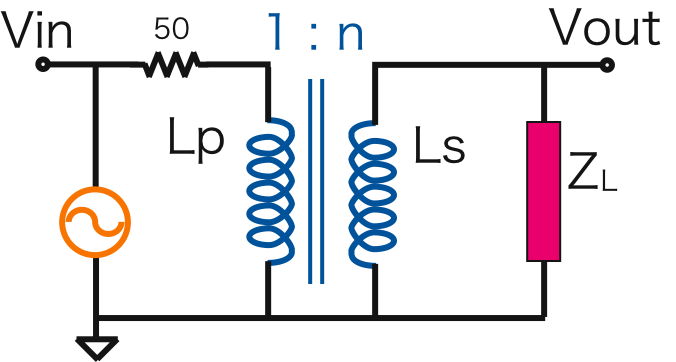
The principle of impedance matching with transformer is explained as follower. At first consider the simple case, a transformer with load impedance ZL. The figure below shows the schematic of the circuit with the transformer.
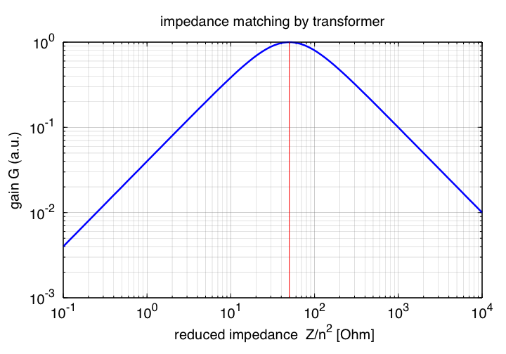
In the figure above, Lp represents the inductance of primary coil, and Ls represents that of secondary coil. Generally the signal source has an output impedance, which is 50 Ohm in this case. One of the most important role of the transformer is changing the impedance. For example the load impedance looks reduced by 1/n2 if we look at the impedance from the primary coil side. Thus the source voltage Vin will be shared by 50 Ohm and reduced load impedance ZL/n2 in series, then the output voltage Vout will be expressed as
- attachment:equation1.png
Note that the coefficient n directly indicates the step-up gain. The total gain G will get its maximum when the impedance matching is satisfied. Namely,
- attachment:equation2.png
- is the condition of the impedance matching. In this case the maximum gain is described as;
- attachment:equation3.png
- In summary the things we should say about the gain and the impedance matching are
- in order to maximize the gain, impedance matching is required
- under the impedance matched condition, we can increase the gain by increasing the load impedance.
- Those are the reasons why impedance matching is so important. Moreover there are another merits in impedance matching. An impedance matched system can avoid the reflection of signal, which might be harmful for some circuits, and avoid the standing wave, which makes behavior of the circuit more complicated.
2.2 LC resonant circuit
In this section the LC resonant circuit is introduced because multi-resonant circuit can be essentially considered as the set of the LC resonant circuit. Now consider the circuit with an inductor L and a capacitor C in parallel.
The impedance of L has a phase angle of 90 deg from real axis, and that of C is -90 deg. As frequency goes up the amplitude of impedance for L increase.
- attachment:equation6.png
- The circuit resonates when the angular frequency is
- attachment:equation5.png ,
- where the denominator gets to completely zero. An interesting thing will be found if you look at the impedance in frequency-impedance domain (like a bode plot).
There are two solid line, one with f1 dependence represents impedance of L, the other solid line with 'f'-1 represents that of C. Then the resonance occurred where those two lines are crossing. This phenomenon physically indicates a [. According to equation above, the resonant impedance goes to infinity thanks to have a pure imaginary number. However if impedance of L and C have an extra real part, the cancellation does not complete and eventually the resonant impedance is no longer infinite.


2.3 Loss
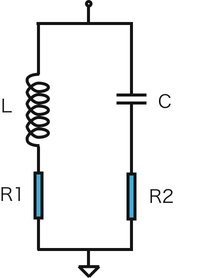
At first think about the parallel LC circuit. In the ideal case, where no losses, impedance can goes up infinitely at the resonant frequency. However in the real circuit Zres has a finite number. The one of the component which makes Zres lower is the loss. Thus we have to think about the effect of loss toward the Zres. Begin with a simple model shown in fig.2, parallel LC resonant circuit with a DC resistance in serial to L and C each.
- In this case the impedance of this circuit is expressed as;
- attachment:equation7.png
Where R1 and R2 is the loss of the inductor and the capacitor respectively. At the resonance the impedance can be approximately described as;
- attachment:equation9.png
Here R represents the sum of each loss, namely R=R1+R2.
From this relation we can find the following general prescriptions to make a high Zres.
- bigger L
- smaller C
- smaller loss
- These are the general recipe for making a good (high impedance) resonant circuit.
2.4 return loss
In the RF domain, usually the reflection of the signal leads to some problems. One of the biggest effects is the return loss. Consider following example situation; a signal generator with the output impedance of 50 Ohm is driving a load composed by a circuit and an EOM.
- In this case the reflection of the signal will occur at the impedance discontinuity point (black dot in the figure above). The reflection coefficient for the voltage of the signal is defined as;
- attachment:equation12.png
Where Z represents the input impedance of the load composed by the circuit and the EOM. Because of this, a part of the generated voltage will be reflected while another part can go through. So that the reflection can reduce the RF power transferred to EOM. This is the principle of the return loss.
- input impedance of the circuit should be close to 50 Ohm in order to minimize the return loss

3. Study of Single resonant circuit
- In order to understand how the circuit works and how losses affects, we started with a single resonant circuit. The circuit is composed by L, C and transformer in parallel.
3.1 EOM
- One of the key component in the circuit is the EOM, which can be dealt as a capacitor electrically. The EOM also has a DC resistance, namely a loss. In the design phase we have to take about this fact.
3.2 design
- Based on the result described above, the single-resonant circuit is designed.
3.2.1 input impedance
- The input impedance of the resonant circuit should be 50 Ohm at desired frequency, otherwise the gain will be decreased. Related to this topics, there is one more thing to take care of. That is the effect from leakage inductance onto the input impedance. If the leakage inductance is larger than the 50 Ohm at the resonant frequency, the leakage inductance will dominate the input impedance and finally degrades the gain.
- The below shows the equivalent circuit of a transformer with the leakage inductance.
Where Le is the leakage inductance and M is the mutual inductance. These are related with the primary (secondary) coil via the coupling coefficient k as (1-k)Ls=Le and M=kLs. In typical transformer k is almost unity like ~ 0.995. The load impedance ZL now appears with reduction by 1/n2. The transformer behind the circuit is the ideal transformer, which only steps up the voltage. Usually M has a much larger impedance than the others, so that we can neglect M as an open. Then the input impedance of this circuit should be
- attachment:equation10.png
At the resonant frequency, ZL/n2 is adjusted to 50 Ohm. However this adjusted impedance will be disturbed by the leakage inductance. So that the requirement for avoiding the effect of the leakages is expressed as;
- attachment:equation11.png
If we put the resonant frequency of 55MHz, Le needs to be less than 72nH. Then assuming the k=0.999, the inductance of the primary coil must be less than 72uH. For summary
- the inductance of the primary coil must be less than 72uH

3.3 optical test
- So far we only think about electrical aspect, here the optical aspect is considered. The motivation of optical test is
3.4 conclusion
- Through whole measurement there are some suggestion for designing better circuit.
4. multiply resonant circuit
4.1 what's difference from single-resonance ?
- Here we consider the difference between multi-resonant and single-resonant. This
4.2 design
- The requirements for the multiply-resonant circuit are follower;
4.3 performance test
- Here we will report the resultant performance of the circuit both in electrical and optical test.
- As we expected....
4.4 conclusion
- We have developed the multiply resonant circuit, which.....
A. impedance measurement
- In this chapter the technique for measuring the impedance by using Network Analyzer (Agilent AG4395A) is explained.
A.1 voltage dividing technique
- Network analyzer is the apparatus basically measure the RF power. In order to measure the impedance of a sample a trick is needed. One of the easy way is that based on the principle of voltage dividing. For example
A.2 impedance test kit
In order to crosscheck the measured impedance data, we took the same data by using a different configuration. We have usually taken the data by using voltage dividing technique described above. Another way to measure the impedance is using AG4395A with the extension kit A4016. This extension kit allows us to directly observe impedance typically from 10-2-106 Ohm. The figure shown below is the comparison of results which taken using these two different configuration. The resonant frequency differs about 10%, it might cause by parasitic capacitor of lead inductance. The significant point is that those two Zres show good agreement within 5% difference.
